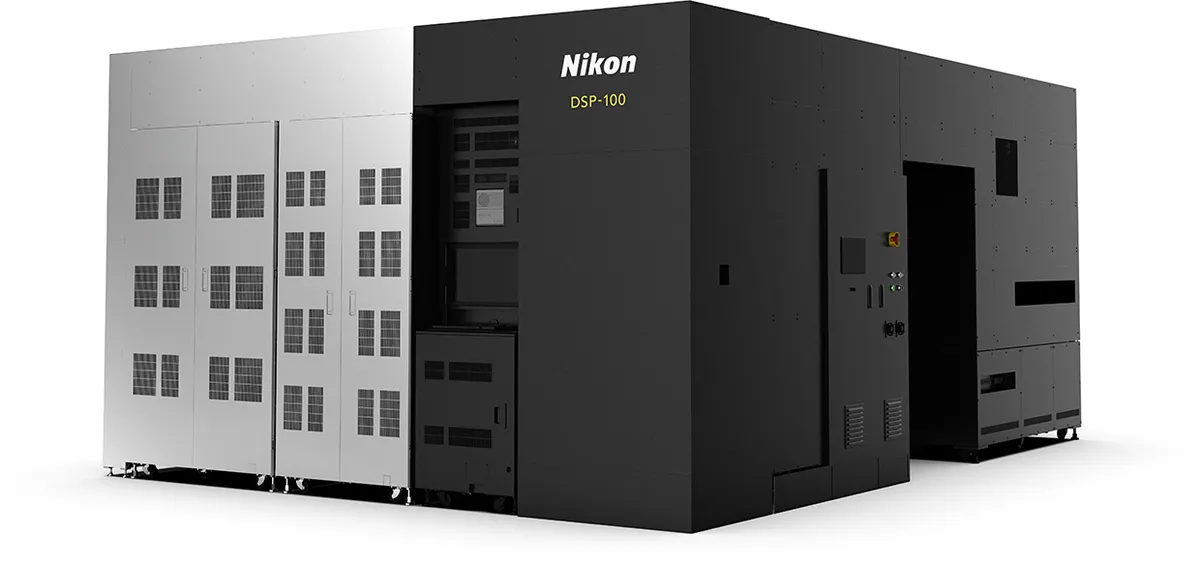
Nikon Corporation is developing a new digital lithography system for semiconductor advanced packaging, targeting 1.5 µm (L/S) resolution and a throughput of 65 panels per hour or better. The system, slated for fiscal year 2027 release, extends Nikon's maskless digital lithography lineup beyond the DSP-100, which delivers 1.0 µm (L/S) resolution and began taking orders in July 2025.
The throughput jump is the primary differentiator. The new system targets more than 30 percent improvement over the DSP-100's 50 panels per hour, based on 510 × 515 mm substrates. What's new here is an explicit resolution tier for customers whose large interposer and FC-BGA substrate processes don't require 1.0 µm line-and-space capability, giving those manufacturers a faster tool matched to their actual process spec.
Like the DSP-100, the system uses maskless architecture, eliminating photomasks and the tooling cost and lead time that come with them. Nikon is also building in an upgrade path. The optical module can be exchanged to restore 1.0 µm (L/S) resolution if process requirements tighten later, without replacing the system outright.
Demand is rising alongside GPU and high-bandwidth memory production tied to generative AI applications. Panel-level packaging has gained ground as chipmakers pursue higher productivity on large substrate formats, but wiring requirements across interposers and FC-BGA substrates vary enough by customer process that a single resolution standard doesn't fit every application. Nikon says input from customers drove the decision to add a second resolution tier. The DSP-100, the company's first digital lithography system, had not yet shipped as of this announcement, with its fiscal year 2026 release still pending.